1 / 5
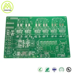
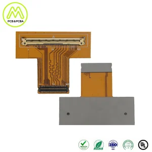
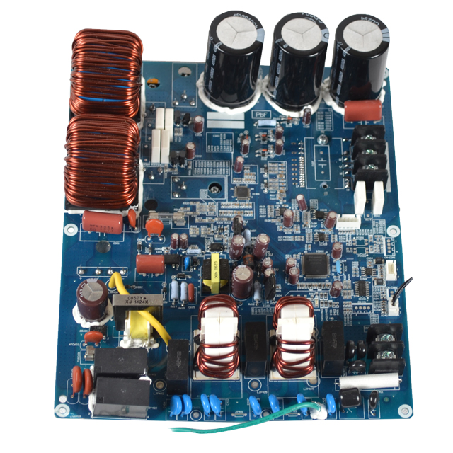
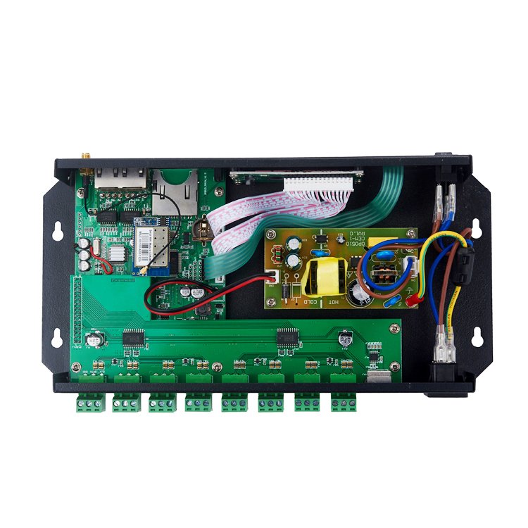
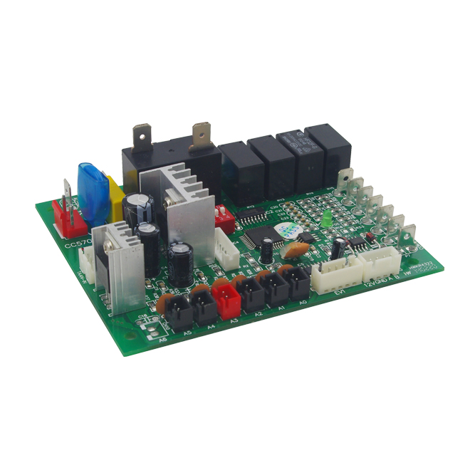
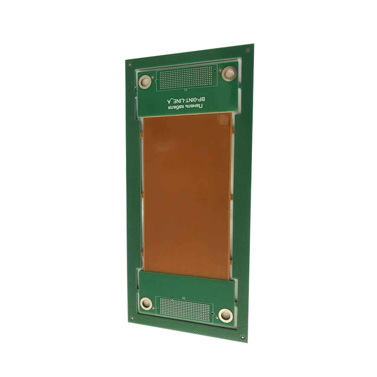
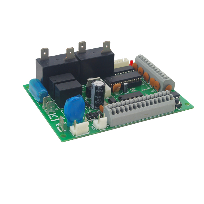
A professional manufacturing enterprise majoring in high-end and multi-layer Printed Circuit Boards. With over 10 years of development, the expert team consists of professionals with no less than 10 years of experience in the PCB field.
| Service Category | Capabilities & Specifications |
|---|---|
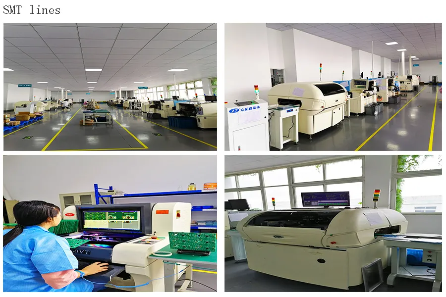
| Assembly Details | SMT and Thru-hole, ISO SMT and DIP lines |
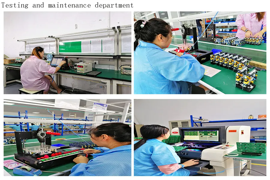
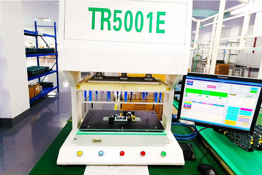
| Testing Services | Testing jig/mold, X-ray Inspection, AOI Test, Functional test |
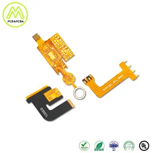
| Panel Size | Min: 0.25*0.25 inches (6*6mm) | Max: 1200*600mm |
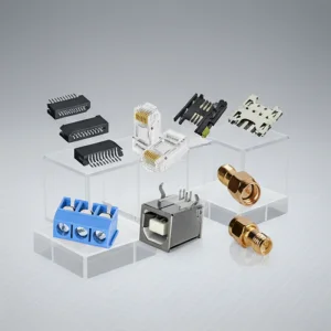
| Component Details | Passive down to 0201, BGA, VFBGA, Leadless Chip Carriers/CSP, Fine Pitch to 0.2mm |
| Process Flow | Drilling > Exposure > Plating > Etching > Punching > E-Testing > SMT > Wave Soldering > Assembly > ICT |

| Pb (Lead) | 0.1% (1000ppm) |
| Hg (Mercury) | 0.1% (1000ppm) |
| Cd (Cadmium) | 0.001% (100ppm) |
| Cr VI+ | 0.1% (1000ppm) |